Applications of M-plane (1-100) 15R-Silicon Carbide and Related Substrates to Eliminate Defects in Epitaxial films
A method of epitaxial growth of SiC substrates for use in semiconductors and other SiC devices
Products can be fabricated using epitaxy; this is a process where a crystalline layer is deposited on a crystalline substrate. Semiconductors can be fabricated through this method. Silicon Carbide (SiC) is a crystalline material existing in various forms (polytypes): that is, these forms differ in physical arrangement but do not vary in stoichiometry. Previously, epitaxial layers have been grown using the polytype 15R-SiC, but this substance is not commercially available in large quantities. There is a need for improved semiconductor material structures and devices, and methods of making them.
This technology is a method of epitaxial growth of a material on a crystalline substrate; a substrate with a crystal plane including a multitude of terraces with step risers that join adjoining terraces is chosen. Every terrace should have a lattice constant which matches a lattice constant of the material; each step riser should have a step height and offset consistent with portions of the material which is nucleating on adjoining terraces. This substrate is prepared by revealing the crystal plane and epitaxially growing the material on the substrate. A single crystal lattice is formed from the merging of portions of material nucleating on adjoining terraces. This method utilizes the 4H-SiC polytype of silicon carbide.
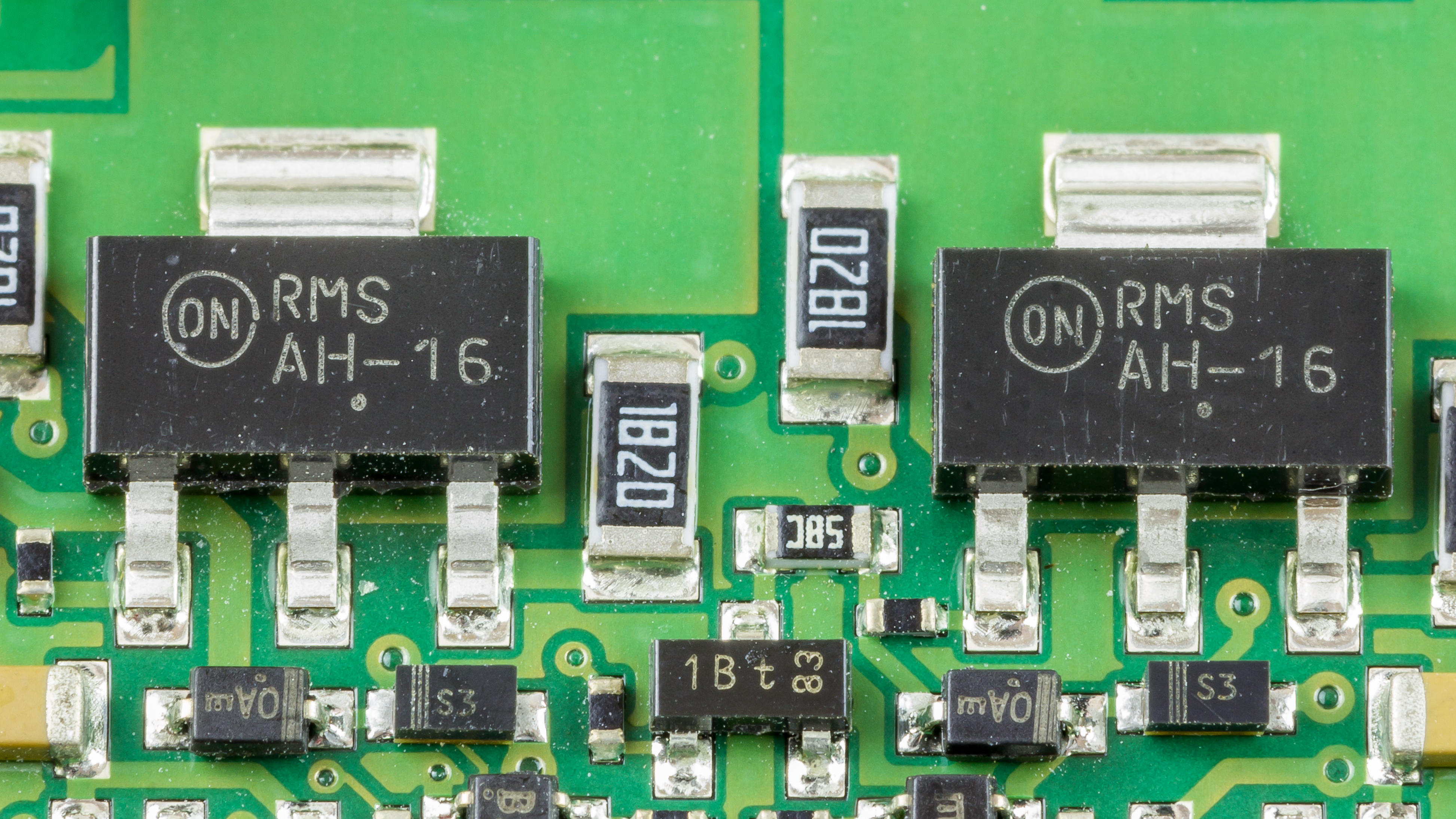 Source: Raimond Spekking, https://commons.wikimedia.org/wiki/File:Fritz!Box_Fon_WLAN_7270_-_ON_Semiconductor_AH-16-3954.jpg, CC BY SA 4.0.
- Utilizes a commercially available polytype of SiC - High crystal quality - Crystal coalescence without defects - Better structural, electrical and optical properties - Semiconductor benefits: - Reduced defect densities - Improved properties - Improved device performance
- Methods of fabricating material structures on a substrate - General SiC devices/semiconductor devices - Icosahedral boron arsenide or boron phosphide neutron detectors - Direct conversion of nuclear energy to electrical energy - 3C-silicon carbide transistors and diodes - 3C?SiC/15R?SiC heterojunction diodes and transistors - Silicon carbide metal oxide semiconductor field effect transistors (MOSFETs) based on alternative epitaxial dielectrics - Detectors and sensors - Light emitting laser diodes - Thermoelectric converters
Patented
[8823014](http://patents.com/us-8823014.html)
Available for licensing.
Licensing,Commercial partner,Development partner
Patent Information:
| App Type |
Country |
Serial No. |
Patent No. |
Patent Status |
File Date |
Issued Date |
Expire Date |
|