Bolometric Sensor with High TCR and Low Resistivity
The invention provides a novel way of operating bolometers in the resistive hysteresis region of a phase-transitioning VO2 film.
Visualization of infrared (IR) radiation is achieved by projecting an IR picture onto a sufficiently large 2D matrix of small microbolometers. Using electrical signals, outputs can be visually displayed, thus creating a pixelated image of the original IR picture. One of the issues resolved by the technology relates to the sensor material and its electrical resistance as a function of temperature.
The technology is a bolometric sensor which uses a thin film of vanadium dioxide exhibiting metal-insulator transition qualities, with an arrangement for controlling and regulating the temperature and resistance of a predetermined point, within a main hysteretic loop of the metal-insulator transition. The sensor uses an electronic readout arrangement to monitor the temperature and resistance of the sensor, thus creating a more accurate and longer lasting sensor for visualization.
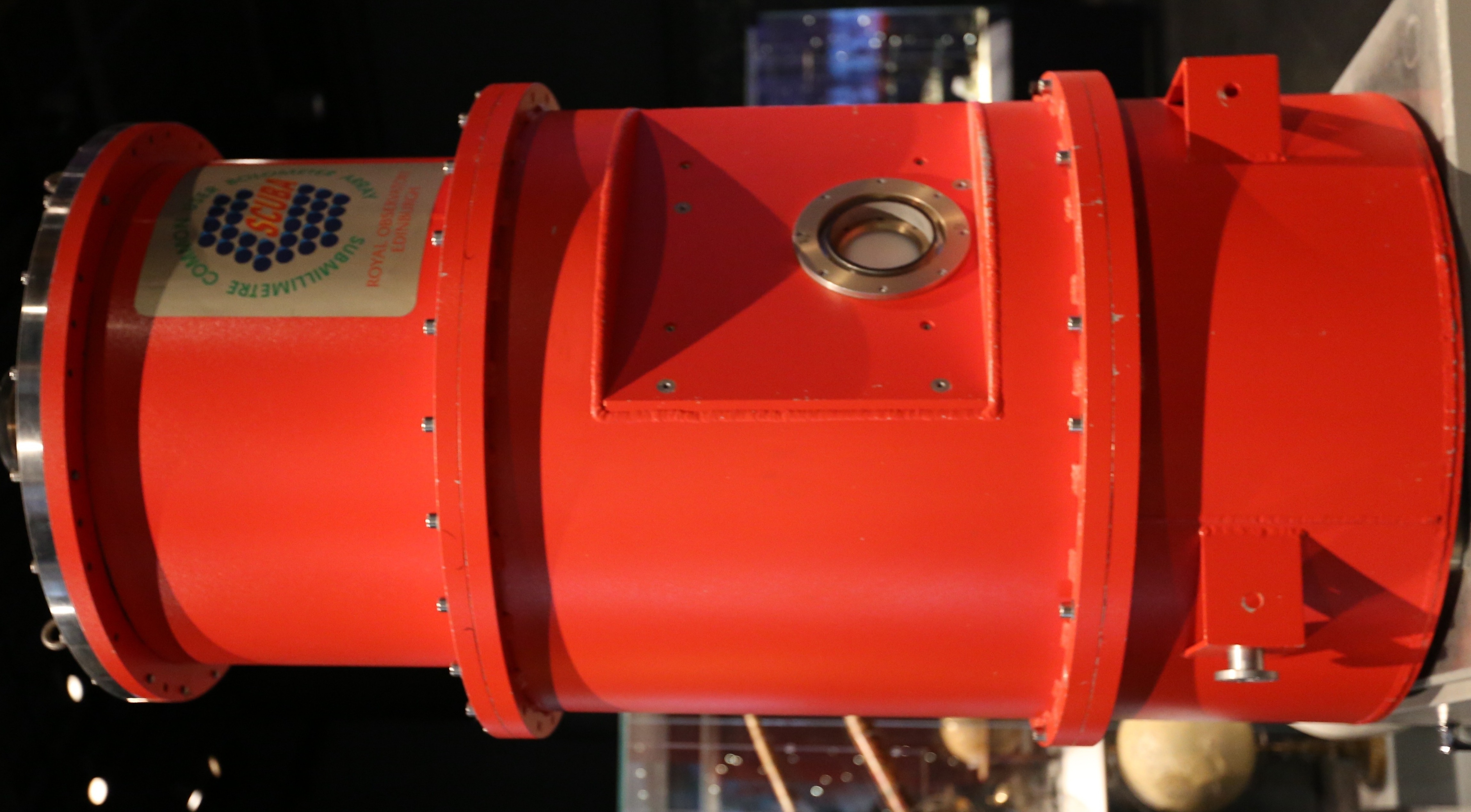
 Source: Geni/Wikimedia, https://commons.wikimedia.org/wiki/File:Submillimetre_Common-User_Bolometer_Array_2013.JPG, CC BY SA 4.0.
- More reliable - More accurate - More communication with user
- Infrared imaging -Bolometry and bolometric sensor design - Focal plane array design
Patented
[8,158,941](https://patents.google.com/patent/US8158941B2/en)
Available for licensing
Development partner,Commercial partner,Licensing
Patent Information:
| App Type |
Country |
Serial No. |
Patent No. |
Patent Status |
File Date |
Issued Date |
Expire Date |
|