Compound Semiconductor Device on Virtual Substrate
Fabrication of infrared photo detectors with high quality and appropriate thicknesses.
The detectors for semi conductors must 1) have a low defect density 2) have complete control over alloy composition of the materials grown. However, traditional infrared photodetectors are created by elements in Group III or V of the periodic table, must fit qualities that will not hinder the capabilities of the semiconductor itself. An example of this problem is radio communication. If the material used to create the photodetector has too much lattice energy, the band gap (eV) able to be detected by the semiconductor can vary.
Fabrication of compound semi-conductor comprising of III-V alloys In and/or Ga, and As and/or Sb. A bulk crystalline substrate having arbitrary lattice constant is obtained for the fabrication of the device comprising non-strained, not relaxed layer of the lattice constant between about 6.1 and 6.5 Angstrom, followed by MBE or MOVPE growth over the said substrate of a transitional layer of AlInGaAsSb material with the composition graded from that matching the lattice constant of the substrate to that providing lattice match with the said non-strained, not relaxed layer of the lattice constant between about 6.1 and 6.5 Angstrom. Layer growth is continued with fixed composition, concluding the said transitional layer and forming a pseudo bulk virtual substrate lattice matched to the said non-strained, not relaxed layer of the lattice constant.
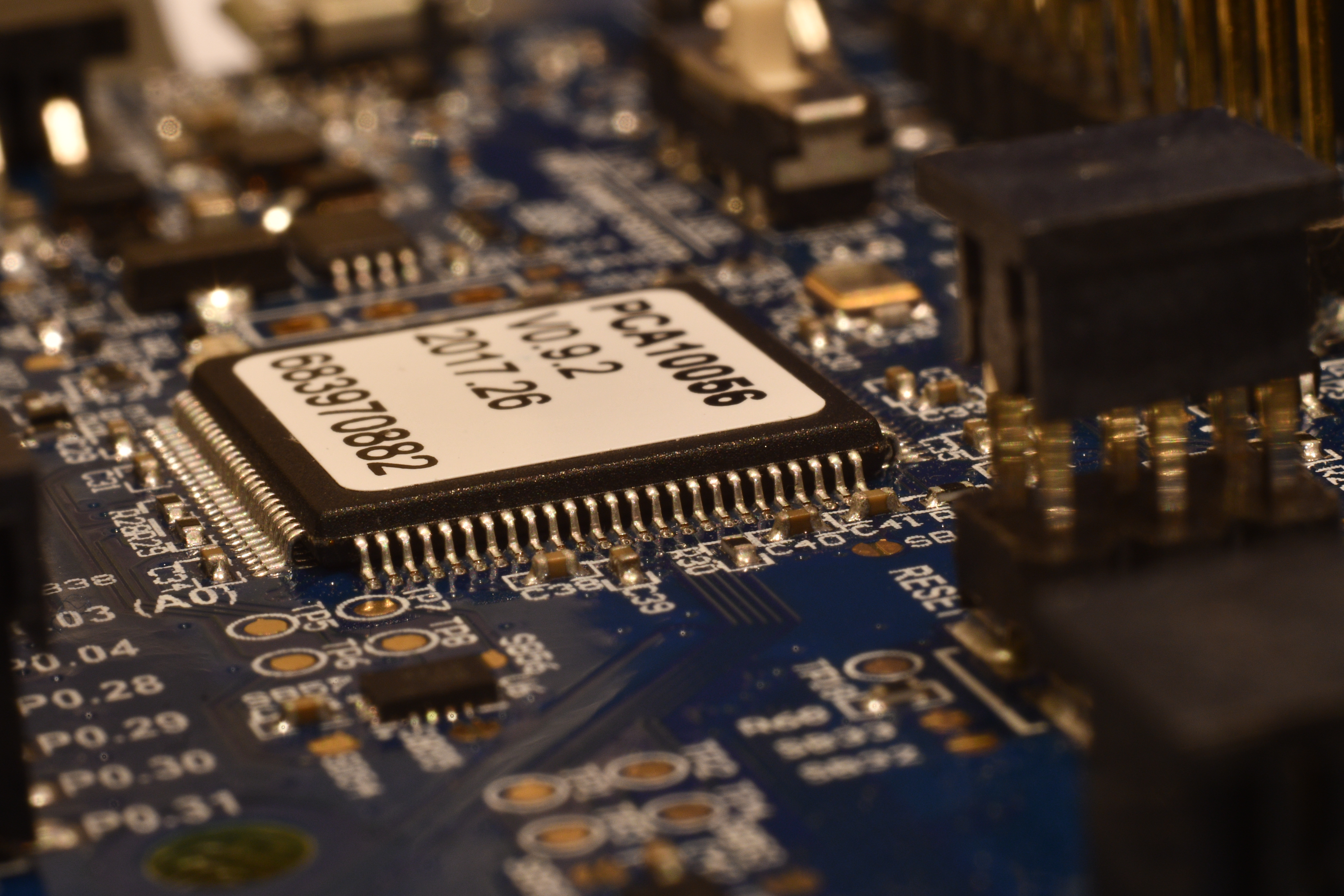
 Please note, header image is purely illustrative. Source: maticulous, Flickr, CC BY 2.0.
- More Accurate - Lower Defect Density - Easier to Produce - More Control
- Barrier Diodes - Semiconductors - Microelectronics
Patented
9065000
Available for licensing.
Development partner,Commercial partner,Licensing
Patent Information:
| App Type |
Country |
Serial No. |
Patent No. |
Patent Status |
File Date |
Issued Date |
Expire Date |
|