Fabrication of Surface Textures by Ion Implantation for Antireflection of Silicon Crystals
A more effective method of texturing silicon surfaces, such as solar cells, to create an antireflective coating.
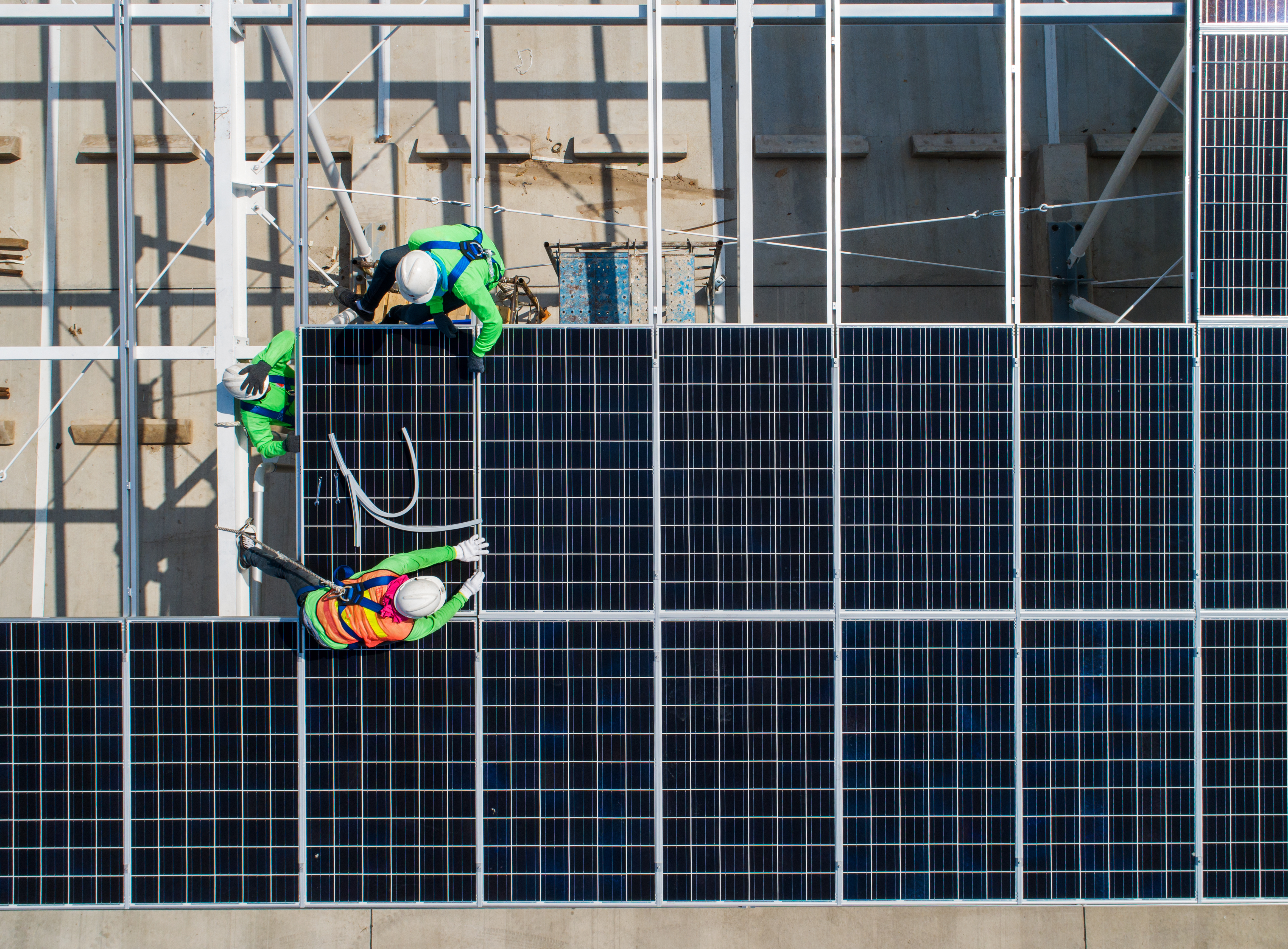
Solar panels rely on photons from sunlight to work. The more sunlight the cells absorb, the more electricity they can produce. But bare silicon cells have very low efficiencies and as much as 30% of light can reflect off its surface before being absorbed. To combat this, manufacturers may texture the surface to interfere with light reflectance. They also add a thin layer of antireflective coating onto the cells to increase the amount of light that can be absorbed. But most are quarter wavelength thin films that reduce light reflection for only a narrow range of wavelengths and incident angles. Continued antireflective improvements are needed to increase solar cell performance.
Creating textured surface structures is one method for improving light absorption in solar cells. Chemical etching is used to form antireflective structures, such as pyramids, but this approach can't be used with thin film solar cells. New approaches producing other structures at depths of a few microns are extremely efficient, but fabrication is costly and complicated. This new approach from SUNY Polytechnic Institute researchers uses co-implantation of hydrogen ions and heavy element ions (argon, krypton, xenon, silicon, and germanium) in a thermal annealing process to create novel textured surfaces. The process is cost effective and utilizes existing semiconductor ion implantation fabrication equipment.
Advantages of this technology include:
- Utilizes existing semiconductor ion implantation fabrication equipment.
- Reduces the number of steps required for ion implantation and is cost-effective to employ.
- Can prevent light reflectance at high rates, up to 95% in some cases.
The primary application for this technology is thin film solar cells, but it could also be beneficial in reducing light reflectance in optical equipment such as cameras, or optical components of medical or other equipment.
Patented, US 9,231,061 Fabrication of surface textures by ion implantation for antireflection of silicon crystals
Technology Readiness Level (TRL) 4: Technology validated in lab.
This technology is available for licensing and could potentially be licensed to companies that manufacture silicon solar cells. Significant growth is expected in the solar power industry over the next decade. For example, the thin film solar cell market is projected to grow to $12.3B by 2025. And the global market for solar energy is expected to reach $220B by 2026.
Patent Information:
| App Type |
Country |
Serial No. |
Patent No. |
Patent Status |
File Date |
Issued Date |
Expire Date |
|