Gas-phase Polymerization for Adhesive Bonding and Packaging Applications
Provides solvent-free bonding of substrates for manufacturing electronic components.
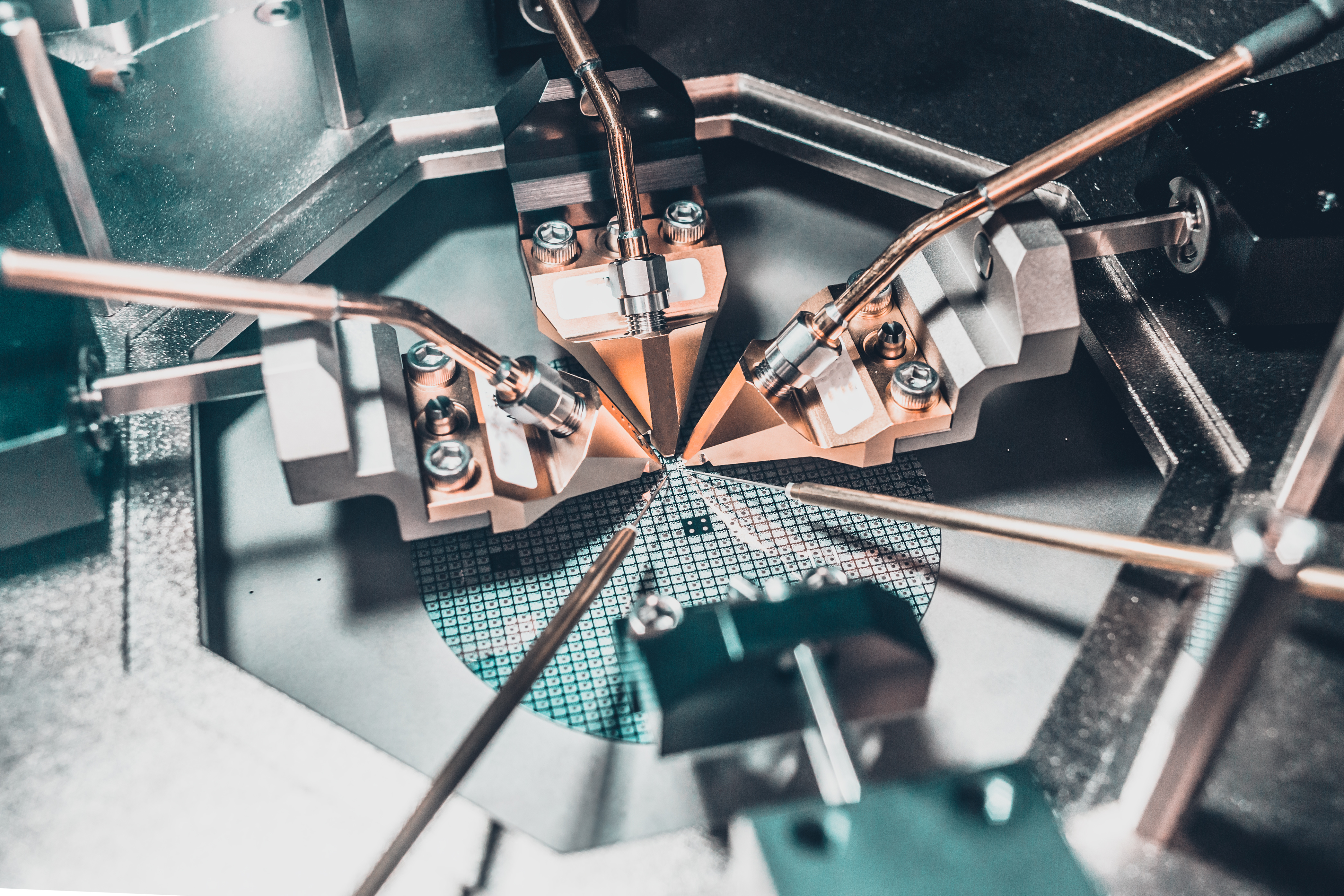
Wafer bonding is a microelectromechanical (MEMS), nanoelectromechanical (NEMS), microelectronic, and/or optoelectronic packaging technology for mechanically stable and hermetically sealed device encapsulation. A number of wafer bonding methods have been developed, including adhesive bonding and others. Adhesive wafer bonding has the advantage of being a relatively low temperature technique that does not require application of electric voltage or current. Adhesive wafer bonding is commonly performed by applying an organic adhesive on one or both substrates. This requires the adhesive to be dissolved in solvent. This has a significant drawback of lacking adequate control resulting in uneven distribution of the adhesive, outgassing of solvents, and delamination and wrinkling upon solvent bake/annealing.
This SUNY Polytechnic Institute technology provides a method for solvent-free bonding of substrates, using a novel technique called initiated chemical vapor deposition (iCVD). This low-temperature method allows deposition of thin polymer films on virtually any material. iCVD is ideal for substrates that are thermally or chemically sensitive. The overall process includes: 1. Depositing a polymeric film on a first surface of a first substrate and optionally depositing a polymeric film on a first surface of a second substrate. 2. (Optional) Aging each substrate comprising a deposited polymeric film at a temperature above the glass transition temperature of the deposited polymeric film until the desired amount of monomers and/or short-chain polymers in the polymeric film is released. 3. Bonding the first substrate to the second substrate by contacting the first surface of the first substrate with the first surface of the second substrate.
- Works with substrates that are thermally and/or chemically sensitive.
- Does not require application of electric voltage/current.
- Controls distribution of the adhesive.
- Avoids outgassing of solvents.
- Avoids delamination and wrinkling.
Manufacture of integrated circuits (IC), including:
- Wafer Level Packaging (WLP)
- System in Package (SiP)
- Three-dimensional (3D) integration
This technology is protected by US Patent 9,505,954 B2, Solvent-Less Adhesive Bonding.
Technology Readiness Level (TRL) 4: Technology validated in lab
This technology is available for licensing and would be of interest to any organization involved in manufacturing integrated circuits, including:
- Chip manufacturers
- Electronic component manufacturers (MEMS, NEMS, and so on)
- Electronic equipment manufacturers
Patent Information:
| App Type |
Country |
Serial No. |
Patent No. |
Patent Status |
File Date |
Issued Date |
Expire Date |
|