In-situ Quantum Dot Growth on Carbon Nanotubes
Carbon nanotube technology with precise control of optical and electronic properties of the resulting device.
There are significant shortcomings of current methods by which to modify the physical properties of nanotubes. For example, there has been poor control over the surface coverage and degree of clustering of nanocrystals on nanotubes. The surface coverage and clustering directly affect the physical properties of the resulting nanotube. Thus, current methods do not allow for precise control of the physical properties of nanotubes. Current methods of producing heterostructures are not amenable to controllably arranging nanotubes into well-defined supramolecular configurations. That is, the resulting heterostructures are primarily unorganized, discrete one-dimensional ?ball-and-stick? structures. Such structures are difficult to organize into orderly assemblies which are necessary for nanoscale integrated systems.
Researchers at Stony Brook University have generated carbon nanotube-nanocrystal heterostructures using a number of different chemical _in situ_ strategies, without the use of intermediary linkers. These heterostructures are novel and critical for the generation of molecular-scale electronic devices because each component of the heterostructure is intrinsically configurable. That is, the size of each nanocrystal or nanotube can be altered in a rational manner, with implications for the optical and electronic properties of the resulting device.
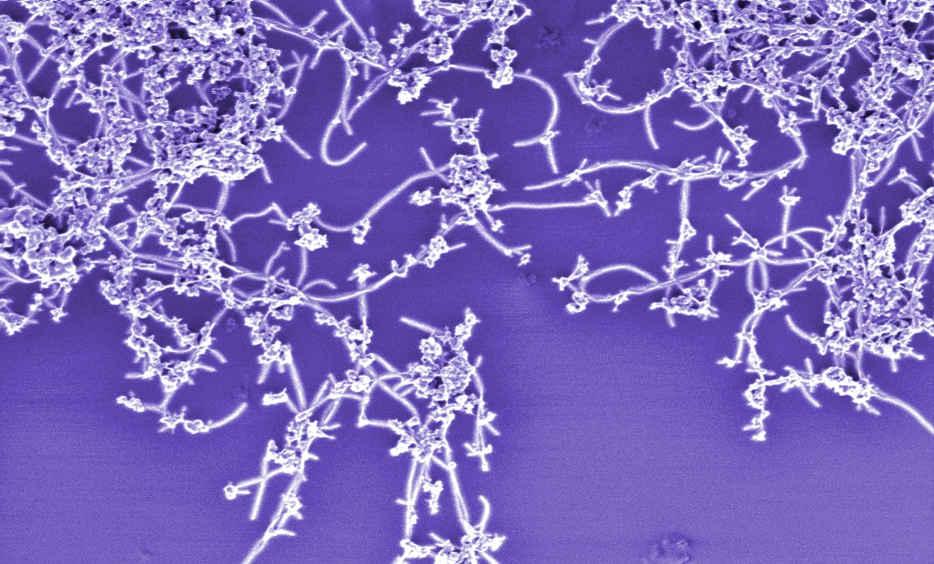 Please note, header image is purely illustrative. Source: National Institute of Standards and Technology, Public Domain Files, public domain
- Single-step synthesis of novel nanotube-nanocrystal assembly is robust and avoids the use of linkers. - Potential of tailoring individual physical, electronic, and chemical properties of single walled carbon nanotubes (SWNTs) and nanocrystals, which is important for molecular electronic and molecular scale devices.
Such integrated systems are required for applications such as: - High-efficiency computing - High-density data storage media - Light harvesting in photovoltaic cells - Lightweight, high-strength textiles - Microelectromechanical devices - Supersensitive sensors - Drug delivery agents
Patented
7189455
Available for Licensing. 7700
Development partner,Commercial partner,Licensing
Patent Information:
| App Type |
Country |
Serial No. |
Patent No. |
Patent Status |
File Date |
Issued Date |
Expire Date |
|