Large-Area PIN Diode with Reduced Capacitance
Novel design of PIN diode that simultaneously has a low capacitance and a large area of effective collection of photo-generated charge
It is highly desirable to implement a PIN diode that collects light from the same area but has a substantially lower capacitance, so that the sensitivity threshold can be greatly improved. The diode capacitance is a key parameter that governs the noise in the front-end amplifier circuit, which is mainly associated with the thermal and flicker noise of the input transistor. The input transistor dominates the noise introduced by readout electronics due to signal amplification in the preamplifier stage. Hence its optimization provides optimal sensitivity.
A novel PIN diode design that simultaneously has a low capacitance and a large area of effective collection of photo-generated charge. The diode capacitance is a key parameter that governs the noise in the front-end amplifier circuit and therefore its reduction provides optimal sensitivity.
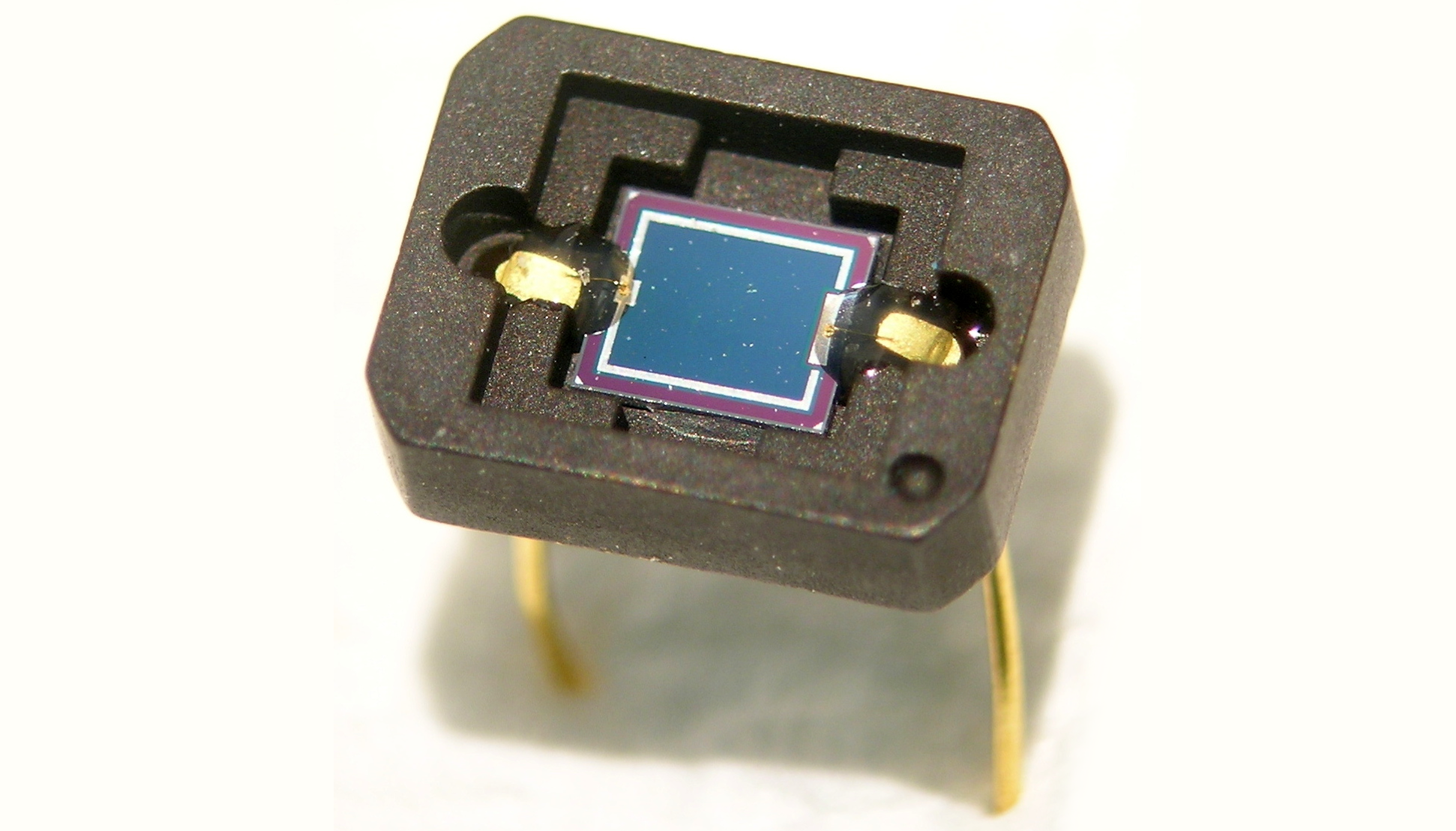 Please note, header image is purely illustrative. Source: John Maushammer, Wikimedia Commons, CC BY-SA 2.5, edited.
The exceptional sensitivity resulting from the capacitance reduction, with no reduction in the collection volume, should be useful for a variety of imaging systems that must be sensitive to low levels of radiation.
The inventive diode will be useful as a pixel in imaging systems that require high sensitivity to low levels of radiation.
Patented
8084838
Available for License.
Licensing
Patent Information:
| App Type |
Country |
Serial No. |
Patent No. |
Patent Status |
File Date |
Issued Date |
Expire Date |
|