Metal Phosphate Nanostructures
A method for producing crystalline metal sulfide nanostructures using a porous membrane and separate metal and sulfur precursor solutions
Recently, high-quality semiconducting nanostructures have been considered as model systems for transporting electrons and optical excitations efficiently. Semiconducting nanowires (made of metal sulfide and rare-earth phosphate nanostructures) are being used as components for several nanoscale energy-conversion, photonic, and electro-optical devices. There are challenges associated with achieving a controlled synthesis of semiconducting nanowires with replicable morphology, crystallinity, chemical composition, and monodispersity. Traditional methods of synthesizing these nanostructures are usually either polycrystalline or require an additional annealing step at a high temperature. Past treatments have involved reactions in an autoclave, usually under anomalous pH conditions, at a relatively high temperature, and reaction times as high as several days. A synthesis method is needed to overcome high temperatures, costly equipment, the production of potentially toxic byproducts, the utilization of costly catalysts and performance-altering capping agents, and the polycrystallinity of the final product.
For the metal sulfide nanostructure, a porous membrane is positioned between a metal precursor solution and a sulfur precursor solution. The porous membrane allows the metal cations in solution and sulfur ions in solution to react, producing a crystalline metal sulfide nanostructure. Here, the metal is a transition metal or a Group IV metal; some examples are copper, lead, cadmium, iron, manganese, cobalt, nickel, zinc, magnesium, tin, germanium, or mixtures of these. The process is similar for a rare earth phosphate nanostructure; again, two precursor solutions are separated by a porous membrane. One is a rare earth metal precursor solution, and the other is a phosphate precursor solution. The membrane allows metal cations from the rare earth metal precursor solution to react with phosphate ions from the phosphate precursor solution. This creates a crystalline rare earth phosphate nanostructure. The rare earth metal, for example, can be cerium, lanthanum, terbium, or samarium, or mixtures of these. Also, this method includes doping the rare earth metal solution with a different rare earth metal; this is the preferred option.
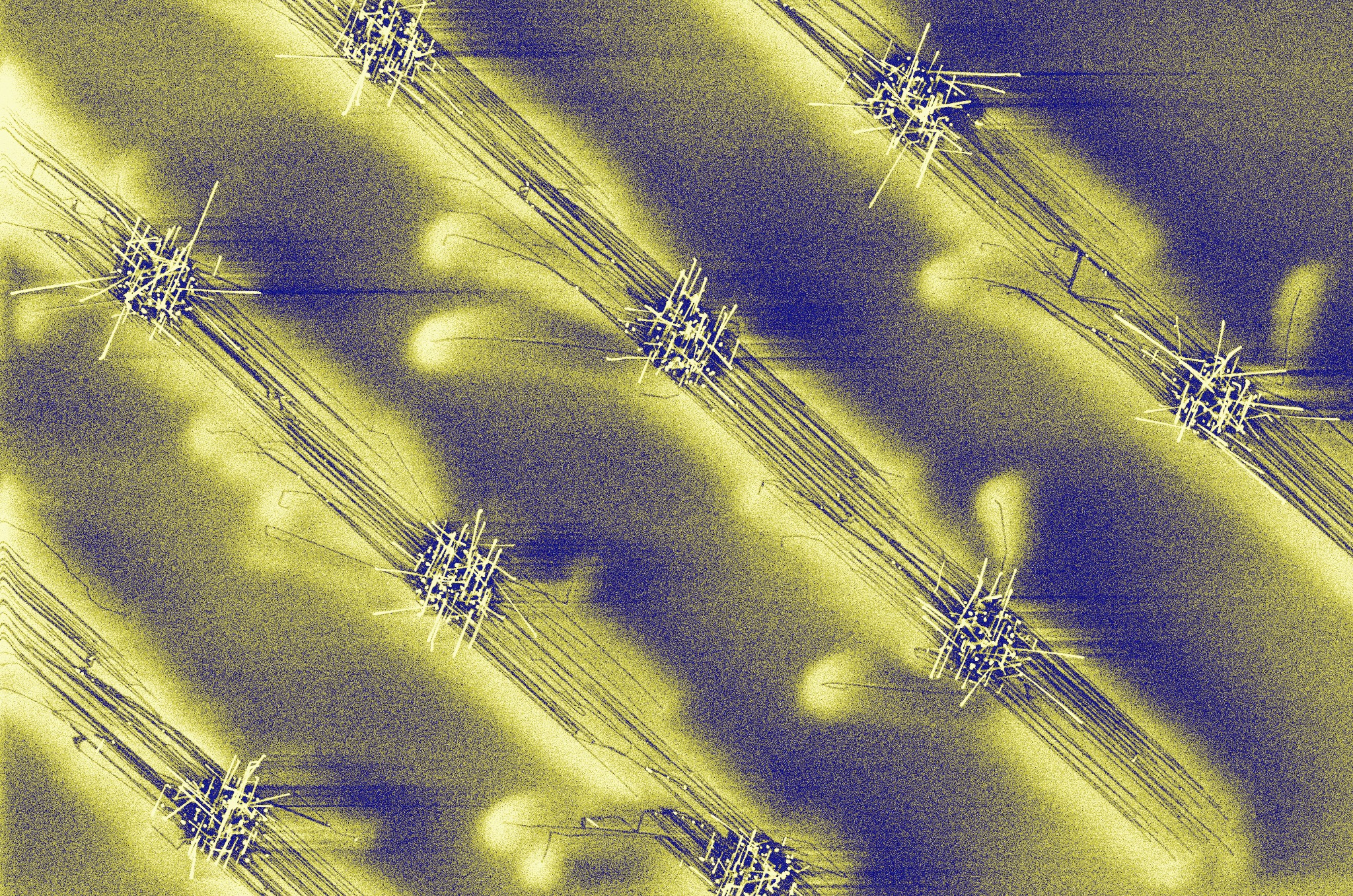
 Please note, header image is purely illustrative. Source: National Institute of Standards and Technology, Flickr, public domain.
- Provides: - preparation of discrete, individual motifs - preparation of arrays of crystalline and pure semiconducting metal sulfide nanowires, generated through a cost-effective, simplistic, and ambient modified template technique - a facile, room-temperature template-directed synthetic route towards the production of distinctive morphologies - High purity, high-aspect-ratio, single crystalline ultrathin nanowires - Sheaf-like nanowire bundles of rare earth phosphates at room temperature - The ultrathin nanowires are fabricated easily on a large scale (greater than 500 mg per lab run, which was previously difficult to achieve with traditional methods) - A wide array of metals are possibilities for use in precursor solutions
- Field-effect transistors - Light-emitting diodes - Logic gates - Lasers - Wave guides - Solar cells - Electronic circuits - Rare-Earth phosphate ultrathin nanowires can be used as fluorescent labels for non-toxic_in vivo_bioimaging (which has not been previously demonstrated as a possibility)
Patented
8721923 9377464
Available for licensing.
Development partner,Commercial partner,Licensing
![]()
Patent Information:
| App Type |
Country |
Serial No. |
Patent No. |
Patent Status |
File Date |
Issued Date |
Expire Date |
|