Optoelectronic Devices Based on Thin Single-Crystalline Semiconductor Films and Non-Epitaxial Optical Cavities
A novel nanoscale optoelectronic device comprising ultrathin materials with single-crystalline quality providing a strong light-matter interaction with high photon absorption and quantum efficiency.
Miniaturization of optoelectronic devices offers tremendous performance gain. As the volume of photoactive material decreases, optoelectronic performance improves, including the operation speed, the signal-to-noise ratio, and the internal quantum efficiency. Over the past decades, researchers have managed to reduce the volume of photoactive materials in solar cells and photodetectors by orders of magnitude. However, two issues arise when one continues to thin down the photoactive layers to the nanometer scale (for example, <50 nm). First, light-matter interaction becomes weak, resulting in incomplete photon absorption and low quantum efficiency. Second, it is difficult to obtain ultrathin materials with single-crystalline quality.
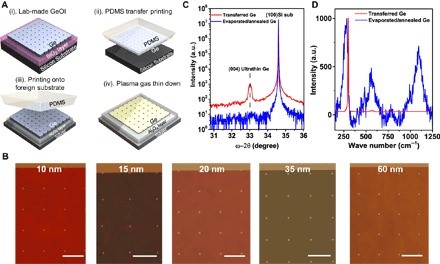
This is a novel nanoscale optoelectronic device with ultrathin materials with single-crystalline quality providing a strong light-matter interaction with high photon absorption and quantum efficiency. It uses conventional bulk semiconductor wafers, such as Si, Ge and GaAs, to realize single-crystalline films on foreign substrates that are designed for enhanced light-matter interactions. A high-yield and high-throughput method is used to demonstrate nanometer-thin photodetectors with significantly enhanced light absorption based on nanocavity interference mechanism. These single-crystalline nanomembrane photodetectors also exhibit unique optoelectronic properties such as the strong field effect and spectral selectivity.

Miniaturization of optoelectronic devices offers tremendous performance gain. As the volume of photoactive material decreases, optoelectronic performance improves, including the operation speed, the signal-to-noise ratio, and the internal quantum efficiency.
Optoelectronic devices
US patent application 15/612,187 filed 6/2/2017 US20180351024A1
Prototype demonstration.
Available for licensing.
Sci Adv. 2017 Jul; 3(7): e1602783
Patent Information:
| App Type |
Country |
Serial No. |
Patent No. |
Patent Status |
File Date |
Issued Date |
Expire Date |
|