Power Module Design for 20 kV Diamond Photoconductive Semiconductor Switch
Modern power grid protection necessitates circuit breakers capable of rapid fault isolation to prevent systemic damage, yet traditional solid-state technologies face significant trade-offs between switching speed and voltage handling. Photoconductive Semiconductor Switches (PCSS) offer a promising alternative due to their superior dv/dt capabilities and high power density; however, integrating these devices into industrial systems presents severe packaging hurdles. Specifically, operating at levels such as 20 kV introduces intense electric field concentrations at material interfaces, increasing the risk of partial discharge and insulation failure. Furthermore, managing the thermal loads generated during high-current operation while maintaining optical transparency for laser triggering remains a critical bottleneck, as standard encapsulation methods often interfere with the triggering signal or fail to provide adequate electromagnetic interference shielding during high-speed switching events.
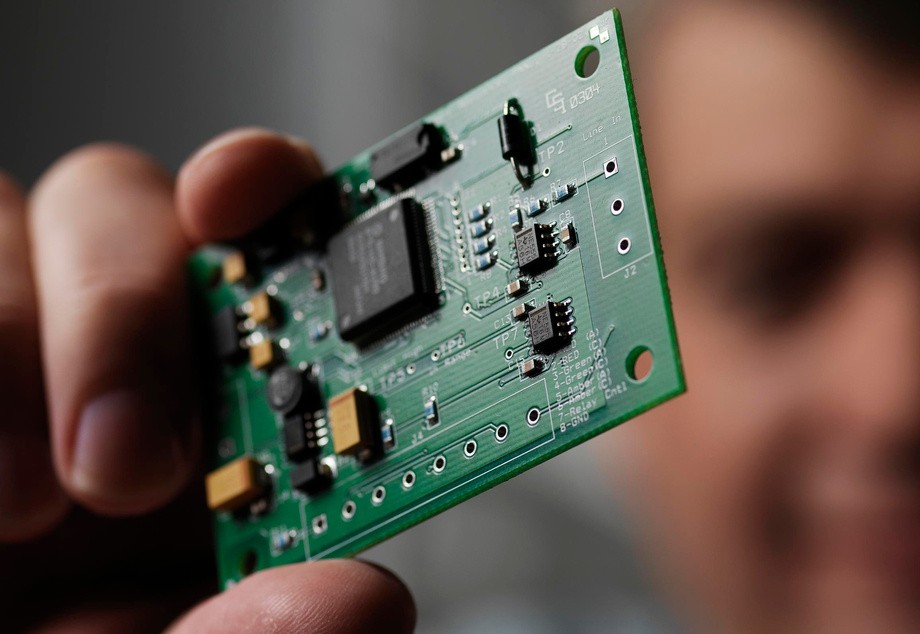
Researchers at Stony Brook University developed a power module utilizing a 3D-printed ceramic substrate featuring a deep cavity to house a 20 kV photoconductive semiconductor switch (PCSS), a configuration designed to minimize electric field concentration and partial discharge risks. To further manage high-voltage stress, an auxiliary diamond insulation layer is inserted between the PCSS die and the substrate for electric field grading and reduced parasitic capacitance. The assembly includes internal blocking walls that segment the silicone gel encapsulation, maintaining a thin layer over a central optical window to ensure unobstructed laser triggering while providing full insulation for the surrounding components. Electrical connectivity is achieved through wire or ribbon bonding to metal connectors, optimized for low inductance and resistance to support high-speed switching and thermal dissipation.
https://commons.wikimedia.org/wiki/File:U.S._Department_of_Energy_-_Science_-_395_027_001_(9578326584).jpg, public domain.
- Superior Switching Speed and Voltage Blocking
- Mitigation of Partial Discharge at Triple Points
- Optimized Optical Triggering Efficiency
- Reduced Parasitic Capacitance and Electromagnetic Interference
- Power Grid Infrastructure and Protection
- Advanced Pulsed Power Systems
Provisional Application Filed
Prototype and Test Data Available
Available
Development partner - Commercial partner - Licensing
Patent Information:
| App Type |
Country |
Serial No. |
Patent No. |
Patent Status |
File Date |
Issued Date |
Expire Date |
|