Selective Metallic Tube Reactivity in the Solution-Phase Osmylation of Single-Walled Carbon Nanotubes
Method of differentiating metallic carbon nanotubes from semiconducting carbon nanotubes
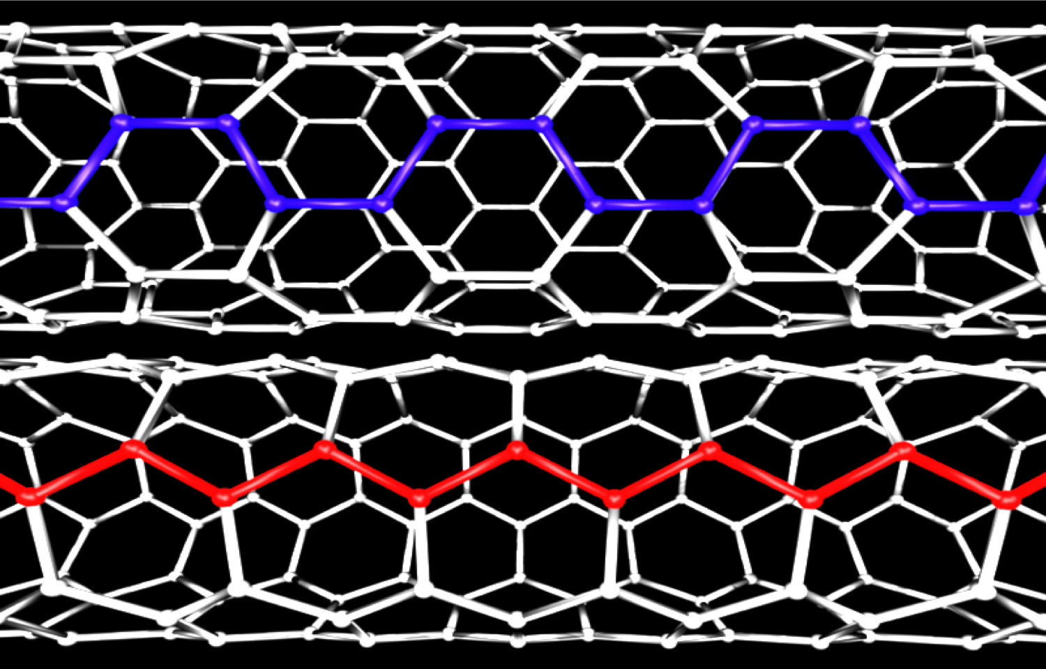
Since their discovery in the early 1990s, carbon nanotubes have been the focus of intense study due to their very desirable and unique combination of physical properties. They are chemically inert, thermally stable, highly strong, lightweight, flexible and electrically conductive. In fact, carbon nanotubes may potentially be stiffer and stronger than any other known material. Noncovalent and covalent sidewall chemistry to probe differential reactivity in metallic and semiconducting nanotubes has been used to affect the bulk separation of nanotubes. However, such noncovalent methods are not efficient; and such covalent methods require nanotubes to be individualized. Accordingly, there remains a need for a simple and efficient method of differentiating between semiconducting and metallic SWNTs which does not require individualization of SWNTs, i.e., which can be performed in bulk.
Nanotube osmylation, based on differential reactivity of nanotube species, holds promise for the selection of nanotubes of particular electronic structure and size, essential for applications such as the development of nanotube-based electrodes as well as advances in molecular electronics. Indeed, the reactivity observed in this work should not only provide the basis for chirality and site-selective nanochemistry and self-assembly applications (such as the fabrication of nanotube-based composites) but also enable a means of altering the known electronic, optical, and mechanical properties of SWNTs in a controllable manner.
 Please note, header images are purely illustrative. Source: Timmymiller, Wikimedia Commons, public domain
-Potential for robust and simple chemical route, without any need for particularly sophisticated equipment, towards separation of metallic and semiconducting nanotubes. This will resolve the key problem/hurdle in the widespread application of carbon nanotubes in electronics by permitting manipulation of tubes according to their electronic structure. -Reactions have been demonstrated in bulk scale, Thus, nondestructive, bulk separation may be achievable. -The observed differences in tube reactivity do not seem to require nanotube individualization.
-Manipulation of tubes according to their electronic structure -Nondestructive, bulk separation may be achievable
Patented
7481990
Available for Licensing.
Licensing
Patent Information:
| App Type |
Country |
Serial No. |
Patent No. |
Patent Status |
File Date |
Issued Date |
Expire Date |
|