Semiconductor Annealing Monitoring
Provides real-time, in-situ monitoring of conductivity change in a doped semiconductor wafer that is being subjected to pulsed microwave annealing.
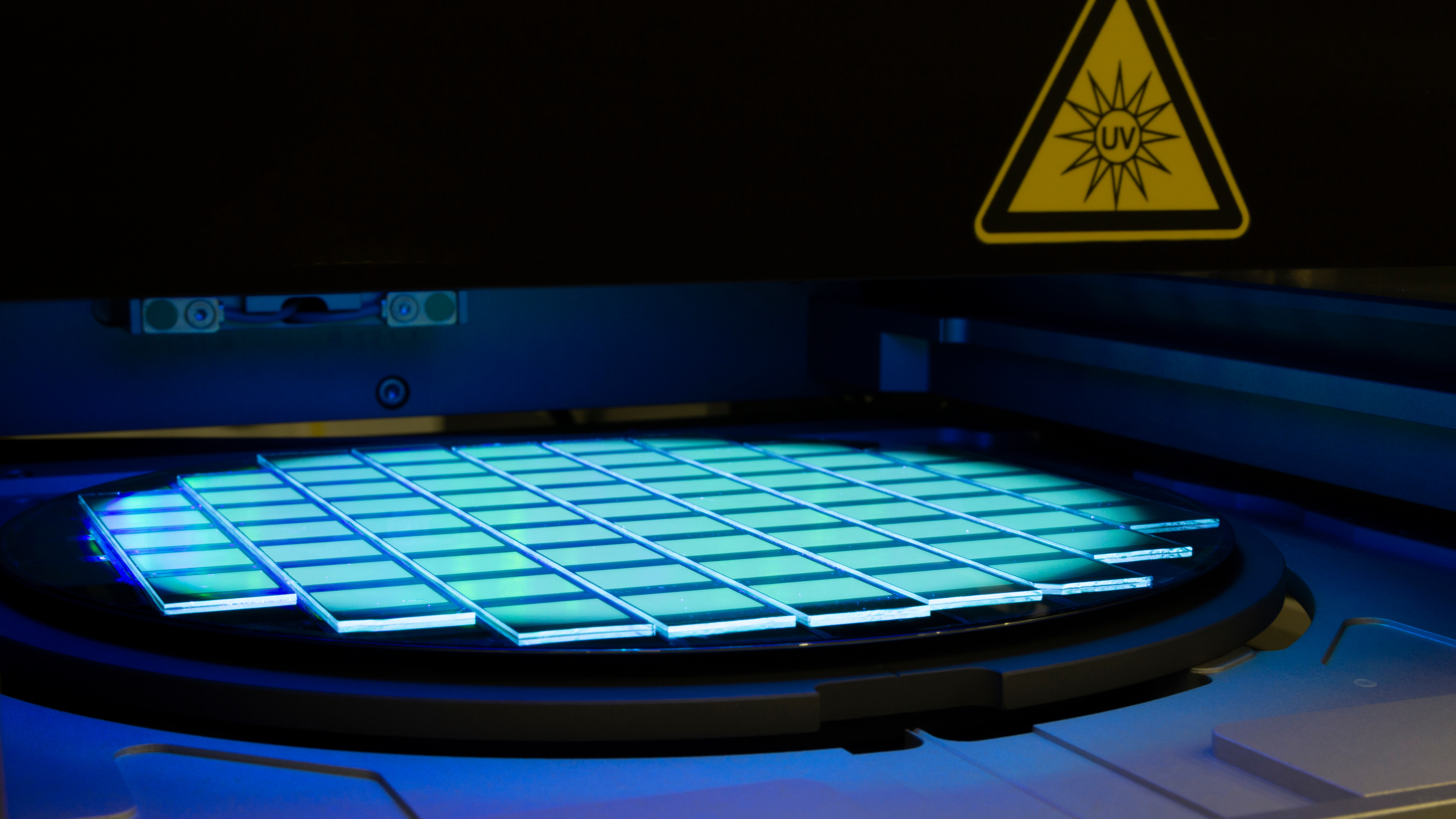
Certain semiconductor wafers are manufactured via a process called doping. During this process, a material (the dopant) is introduced into the semiconductor crystal to change its electrical properties to meet the specifications of the application in which it will be used. During manufacture, doped semiconductor wafers are annealed by applying pulsed microwave energy. The dopants introduced into the crystal may initially be electrically inactive, and become electrically active during annealing. This changes the wafer’s resistivity as the annealing process progresses. At present, annealing is monitored via photovoltage measurement of the wafer surface, a method that requires monitoring the temperature at two surface locations. Ideally, monitoring could take advantage of the fact that change in the material conductivity affects the rate at which microwave energy of a given frequency and electric field strength interacts with the wafer, enabling monitoring of annealing in situ.
This technology is a noncontact, nondestructive monitoring system that detects relative changes in the material’s electrical conductivity in situ during annealing. The system includes a microwave source and remote temperature monitor. The microwave source heats the material, while the monitor detects the rate of temperature change of the workpiece. By comparing the rate of temperature rise as annealing progresses and (by proxy) the changing efficiency of microwave absorption by the material, changes in the material conductivity can be detected. The system can monitor electrical activation of impurities during the progression of a recipe, or used in real time in situ to dynamically change process conditions in response to conductivity change.
Simplicity: This process is simpler that current monitoring techniques. This enables the method to be implemented faster and cheaper.
The primary use of this technology is in-line wafer testing for electrical conductivity changes of semiconductor during microwave annealing.
Patent application filed.
TRL 6 - Technology demonstrated in relevant environment. A working prototype is available for demonstration.
This technology is available for licensing.
This technology could be licensed to any facility that manufactures semiconductors. These include:
- Chips
- IC boards
- Electronic devices
Patent Information:
| App Type |
Country |
Serial No. |
Patent No. |
Patent Status |
File Date |
Issued Date |
Expire Date |
|