Fabrication of highly electrically conducting patterns via inkjet printing
of mussel-inspired organic nano-material
Emerging flexible electronic devices have exhibited significant potential for a wide range of applications, such as sensors, solar cells, batteries, antennas, and displays.
For any flexible electronics application, an essential element is electrically conductive patterning. Solution-based additive manufacturing techniques such as drop-on-demand (DOD) inkjet printing, slot die coating, and gravure printing are being widely investigated to fabricate flexible conductive patterns. DOD inkjet printing is an excellent candidate because it is a material-conservative, low-temperature process and is easily incorporated into large scale roll-to-roll (R2R) manufacturing infrastructures for flexible substrates.
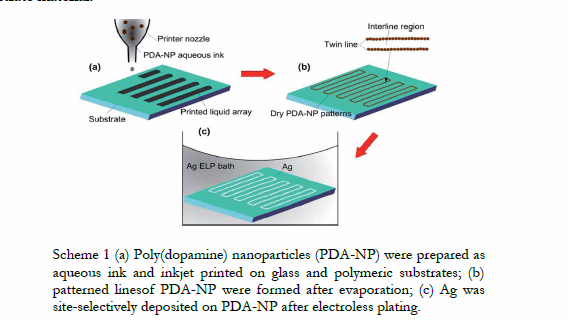
The present invention provides inkjet printing of an aqueous suspension of synthesized mussel-inspired poly(dopamine) nanoparticles. Fine lines of printed nanoparticles have been deposited on both glass and polyethylene terephthalate (PET) substrates by exploiting the coffee ring effect. Deposited particles were then used for site-selective silver/copper metallization via a simple electroless plating process at controlled temperature and plating time. The resulting narrow lines of silver exhibited a resistivity 10.0 times that of bulk silver, and the resulting narrow lines of copper exhibited a resistivity 6.5 times that of bulk copper. Lines on PET retained good electrical and adhesion performance even after many bending cycles. This technique satisfies general requirements of flexible electronics manufacturing – low temperature, low cost, small feature size and good electrical conductivity independent of substrate material.
- Entire process is at low cost and low temperature with minimal environmental footprint
- Achieved structure shows high electrical conductivity independent of substrate material
- Process is transferrable to various material systems and conserves material
- Printed Electronics Manufacturing
- Flexible Electronics.
Patent Information:
| App Type |
Country |
Serial No. |
Patent No. |
Patent Status |
File Date |
Issued Date |
Expire Date |
|